


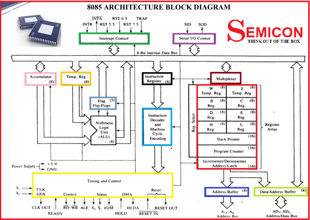
Tổng quan kiến trúc vi xử lý 8085
Vi xử lý 8085 là một vi xử lý 8-bit do Intel phát triển, được sử dụng rộng rãi trong giáo dục và các hệ thống nhúng đơn giản. Sơ đồ khối thể hiện cách các thành phần bên trong phối hợp để xử lý dữ liệu, điều khiển luồng chương trình và giao tiếp với thiết bị ngoại vi.
1. Khối xử lý trung tâm (Data Processing Unit)
A. Accumulator (A)
Là thanh ghi 8-bit trung tâm trong ALU.
Tất cả các phép toán số học và logic đều sử dụng hoặc trả kết quả về Accumulator.
Ví dụ: Lệnh ADD B sẽ cộng nội dung thanh ghi B với A, kết quả lưu lại trong A.
B. Temporary Register
Không truy cập trực tiếp từ phần mềm.
Dùng để lưu tạm dữ liệu trong quá trình thực hiện phép toán, đặc biệt là khi xử lý hai toán hạng.
C. ALU (Arithmetic and Logic Unit)
Thực hiện các phép toán: cộng, trừ, AND, OR, XOR, so sánh.
Kết quả được phản ánh qua các cờ trạng thái (Flags).
D. Flag Flip-Flops
Gồm 5 cờ:
Sign (S): Bit cao nhất của kết quả.
Zero (Z): Kết quả bằng 0.
Auxiliary Carry (AC): Dùng trong các phép toán BCD.
Parity (P): Số bit 1 trong kết quả là chẵn/lẻ.
Carry (CY): Có xảy ra tràn bit hay không.
2. Khối điều khiển và thời gian (Control & Timing Unit)
A. Instruction Register
Lưu trữ mã lệnh đang được thực thi.
Sau khi lệnh được nạp từ bộ nhớ, nó được giữ tại đây để giải mã.
B. Instruction Decoder
Giải mã mã lệnh thành các tín hiệu điều khiển nội bộ.
Ví dụ: Lệnh MOV A, B sẽ tạo tín hiệu để truyền dữ liệu từ B sang A.
C. Timing & Control Unit
Tạo các tín hiệu điều khiển như RD (Read), WR (Write), ALE (Address Latch Enable).
Đồng bộ hóa hoạt động giữa các khối và với bộ nhớ ngoài.
3. Các thanh ghi và bộ đếm
A. General Purpose Registers (B, C, D, E, H, L)
Có thể kết hợp thành cặp: BC, DE, HL để xử lý dữ liệu 16-bit.
HL thường dùng làm thanh ghi trỏ đến địa chỉ bộ nhớ.
B. Program Counter (PC)
Tự động tăng sau mỗi chu kỳ lệnh.
Luôn trỏ đến địa chỉ của lệnh kế tiếp cần thực thi.
C. Stack Pointer (SP)
Quản lý ngăn xếp trong bộ nhớ.
Dùng trong các lệnh CALL, RET, PUSH, POP.
4. Khối giao tiếp ngoại vi
A. Interrupt Control
Hỗ trợ 5 ngắt: TRAP, RST7.5, RST6.5, RST5.5, INTR.
Cho phép vi xử lý tạm dừng chương trình chính để xử lý sự kiện bên ngoài.
B. Serial I/O Control
Giao tiếp nối tiếp qua hai chân: SID (Serial Input Data) và SOD (Serial Output Data).
Dùng trong các ứng dụng truyền nhận dữ liệu đơn giản.
5. Khối đệm địa chỉ và dữ liệu
A. Address Buffer
Tách riêng phần địa chỉ cao (A8–A15) để truy cập bộ nhớ.
B. Address/Data Buffer
Chân A0–A7 vừa dùng để truyền địa chỉ, vừa dùng để truyền dữ liệu (multiplexed).
Cần mạch ngoài để tách địa chỉ và dữ liệu (thường dùng latch).
6. Nguồn và xung nhịp
A. Clock Generator
Tạo xung nhịp từ thạch anh ngoài (thường 6 MHz).
Vi xử lý hoạt động với tần số nội bộ là 3 MHz (do chia đôi).
B. Power Supply
Hoạt động với nguồn 5V.
Có chân RESET để khởi động lại vi xử lý.
7. Tổng kết học thuật
Sơ đồ này không chỉ là bản vẽ kỹ thuật mà còn là “bản đồ tư duy” giúp người học hiểu cách một vi xử lý thực hiện chương trình. Từ việc nạp lệnh, giải mã, xử lý dữ liệu, đến giao tiếp với thiết bị ngoại vi – tất cả đều được thể hiện rõ ràng.
Code Verilog tham khào.
Các module chính trong dự án:
| Tên module | Chức năng chính |
|---|---|
| ALU.v | Thực hiện các phép toán số học và logic |
| RegisterFile.v | Quản lý các thanh ghi đa dụng (B, C, D, E, H, L) |
| IDecoder.v | Giải mã lệnh từ Instruction Register |
| ControlUnit.v | FSM điều khiển luồng thực thi lệnh |
| Memory.v | Mô phỏng bộ nhớ chương trình và dữ liệu |
| MP85.v | Module top-level kết nối tất cả các khối |
| tb_MP85.v | Testbench kiểm thử toàn bộ vi xử lý |
== ALU.v
==============================================================================
`timescale 1ns / 1ps
module ALU (
input alu_enable,
input [3:0] alu_op,
input [7:0] iA, iB, iF,
output reg [7:0] oR,
output reg [7:0] oF,
output reg Flag_read_wrbar
);
// Flag positions
parameter CARRY_F = 0;
parameter PARITY_F = 2;
parameter AUXC_F = 4;
parameter ZERO_F = 6;
parameter SIGN_F = 7;
reg aux_carry_add, aux_carry_sub;
reg [8:0] cmp_result;
wire [8:0] sum, diff;
wire parity;
assign sum = iA + iB + ((alu_op == 4'b0001) ? iF[CARRY_F] : 0); // ADC
assign diff = iA - iB - ((alu_op == 4'b0011) ? iF[CARRY_F] : 0); // SBB
assign parity = ~^oR; // Even parity
always @(*) begin
oF = 0;
oR = 0;
Flag_read_wrbar = 1; // Default: do not write to flags
if(alu_enable) begin
case (alu_op)
4'b0000: begin // ADD
{oF[CARRY_F], oR} = sum;
Flag_read_wrbar = 0;
end
4'b0001: begin // ADC
{oF[CARRY_F], oR} = sum;
Flag_read_wrbar = 0;
end
4'b0010: begin // SUB
{oF[CARRY_F], oR} = diff;
Flag_read_wrbar = 0;
end
4'b0011: begin // SBB
{oF[CARRY_F], oR} = diff;
Flag_read_wrbar = 0;
end
4'b0100: begin // AND
oR = iA & iB;
Flag_read_wrbar = 0;
end
4'b0101: begin // OR
oR = iA | iB;
Flag_read_wrbar = 0;
end
4'b0110: begin // XOR
oR = iA ^ iB;
Flag_read_wrbar = 0;
end
4'b0111: begin // CMP
cmp_result = iA - iB;
oF[CARRY_F] = cmp_result[8];
oF[ZERO_F] = (cmp_result[7:0] == 8'd0);
oF[SIGN_F] = cmp_result[7];
oF[PARITY_F] = ~^cmp_result[7:0];
oF[AUXC_F] = (iA[3:0] < iB[3:0]);
oR = 8'hZZ;
Flag_read_wrbar = 0;
end
4'b1000: begin // INR
oR = iA + 1;
oF[CARRY_F] = iF[CARRY_F];
Flag_read_wrbar = 0;
end
4'b1001: begin // DCR
oR = iA - 1;
oF[CARRY_F] = iF[CARRY_F];
Flag_read_wrbar = 0;
end
default: begin
oR = 8'hzz;
oF = 8'hzz;
end
endcase
end
oF[ZERO_F] = (oR == 0);
if (alu_op != 4'b0111 && alu_op <= 4'b1001) begin
oF[ZERO_F] = (oR == 0);
oF[SIGN_F] = oR[7];
oF[PARITY_F] = parity;
aux_carry_add = ((iA[3:0] + iB[3:0] + (alu_op == 4'b0001 ? iF[CARRY_F] : 0)) > 4'hF);
aux_carry_sub = ((iA[3:0] - iB[3:0] - (alu_op == 4'b0011 ? iF[CARRY_F] : 0)) < 0);
oF[AUXC_F] = (alu_op <= 4'b0001) ? aux_carry_add :
(alu_op <= 4'b0011) ? aux_carry_sub :
0;
end
end
endmodule
==============================================================================
ControlUnit.v
==============================================================================
`timescale 1ns / 1ps
module ControlUnit(
input wire clk,
input wire rst,
input wire decoder_reg_write,
input wire decoder_mem_read,
input wire decoder_mem_write,
input wire decoder_use_alu,
input wire decoder_use_immediate,
input wire decoder_is_branch,
input wire [3:0] decoder_branch_type,
input wire decoder_halt,
input wire [1:0] decoder_inst_length,
input wire [2:0] decoder_src_reg,
input wire [2:0] decoder_dst_reg,
input wire [3:0] decoder_alu_op,
input wire [7:0] mem_out,
input wire[7:0] FLAGS,
input wire decoder_is_mov,
output reg pc_enable,
output reg ir_load,
output reg mar_load,
output reg mar_sel_wz,
output reg mem_read,
output reg mem_write,
output reg reg_write,
output reg alu_enable,
output reg [2:0] latched_src_reg,
output reg [2:0] latched_dst_reg,
output reg [3:0] latched_alu_op,
output reg [7:0] W,
output reg [7:0] Z,
output reg latched_use_imm,
output reg latch_is_mov,
output reg latched_is_branch
);
localparam [2:0] FETCH = 3'b000, DECODE = 3'b001, FETCH_OP1 = 3'b010,
FETCH_OP2 = 3'b011, MEM_RD = 3'b100, EXEC = 3'b101,
WB = 3'b110, HALT = 3'b111;
// Flag positions
parameter CARRY_F = 0;
parameter PARITY_F = 2;
parameter AUXC_F = 4;
parameter ZERO_F = 6;
parameter SIGN_F = 7;
reg [2:0] state;
reg [2:0] t_state;
reg latched_reg_write, latched_mem_read, latched_mem_write, latched_use_alu;
reg latched_halt;
reg [1:0] latched_inst_len;
reg [3:0] latched_branch_type;
always @(posedge clk or posedge rst) begin
if (rst) begin
state <= FETCH;
t_state <= 0;
{pc_enable, ir_load, mar_load, mar_sel_wz, mem_read, mem_write, reg_write, alu_enable,latched_inst_len,latched_src_reg,latched_dst_reg,latched_alu_op,latch_is_mov} <= 0;
latched_use_imm<=0;
latched_branch_type<=0;
end
else begin
case (state)
FETCH: begin
case (t_state)
3'd0: begin mar_sel_wz <= 0; mar_load <= 1; end // Load MAR with PC
3'd1: ; // Wait for MAR to latch
3'd2: begin mem_read <= 1; end
3'd3: ; // Wait for memory
3'd4: begin ir_load <= 1; pc_enable <= 1; end
3'd5:pc_enable <= 0;
endcase
if (t_state == 3'd5) begin
state <= DECODE;
t_state <= 0;
end else t_state <= t_state + 1;
end
DECODE: begin
latched_reg_write <= decoder_reg_write;
latched_mem_read <= decoder_mem_read;
latched_mem_write <= decoder_mem_write;
latched_use_alu <= decoder_use_alu;
latched_use_imm <= decoder_use_immediate;
latched_is_branch <= decoder_is_branch;
latched_halt <= decoder_halt;
latched_inst_len <= decoder_inst_length;
latched_src_reg <= decoder_src_reg;
latched_dst_reg <= decoder_dst_reg;
latched_alu_op <= decoder_alu_op;
latch_is_mov<=decoder_is_mov;
latched_branch_type<=decoder_branch_type;
if (decoder_halt) state <= HALT;
else if (decoder_inst_length == 2'd2) state <= FETCH_OP1;
else if (decoder_inst_length == 2'd3) state <= FETCH_OP1;
else if (decoder_mem_read) state <= MEM_RD;
else if (decoder_use_alu) state <= EXEC;
else state <= WB;
end
FETCH_OP1: begin
case (t_state)
3'd0: begin mar_sel_wz <= 0; mar_load <= 1; end
3'd1: ; // Wait
3'd2: begin mem_read <= 1; end
3'd3: ; // Wait
3'd4: begin Z <= mem_out; pc_enable <= 1; end
3'd5:pc_enable <= 0;
endcase
if (t_state == 3'd5) begin
if (latched_inst_len == 2'd2)
state <= (latched_use_alu ? EXEC : WB);
else
state <= FETCH_OP2;
t_state <= 0;
end else t_state <= t_state + 1;
end
FETCH_OP2: begin
case (t_state)
3'd0: begin mar_sel_wz <= 0; mar_load <= 1; end
3'd1: ; // Wait
3'd2: begin mem_read <= 1; end
3'd3: ; // Wait
3'd4: begin W <= mem_out; pc_enable <= 1; end
3'd5:pc_enable <= 0;
3'd6:;
3'd7:;
endcase
if (t_state == 3'd5) begin
if (latched_is_branch) begin
case (latched_branch_type)
4'b0000: mar_sel_wz <= 1; // JMP (unconditional)
4'b0001: if (FLAGS[ZERO_F]) mar_sel_wz <= 1;
4'b0010: if (!FLAGS[ZERO_F]) mar_sel_wz <= 1;
4'b0011: if (FLAGS[CARRY_F]) mar_sel_wz <= 1;
4'b0100: if (!FLAGS[CARRY_F]) mar_sel_wz <= 1;
4'b0101: if (!FLAGS[SIGN_F]) mar_sel_wz <= 1;
4'b0110: if (FLAGS[SIGN_F]) mar_sel_wz <= 1;
4'b0111: if (FLAGS[PARITY_F]) mar_sel_wz <= 1;
4'b1000: if (!FLAGS[PARITY_F]) mar_sel_wz <= 1;
default: ; // Do nothing special
endcase
end
end
if (t_state == 3'd7) begin
if(latched_is_branch)begin
state <= FETCH; // Always go to FETCH after branch condition is checked
{pc_enable, ir_load, mar_load, mar_sel_wz, mem_read, mem_write, reg_write, alu_enable,latched_inst_len,latched_src_reg,latched_dst_reg,latched_alu_op,latch_is_mov} <= 0;
latched_use_imm<=0;
latched_branch_type<=0;
t_state <= 0;
end
else begin
state <= (latched_mem_read ? MEM_RD : EXEC);
t_state <= 0;
end
end
else begin
t_state <= t_state + 1;
end
end
MEM_RD: begin
case (t_state)
3'd0: begin mar_sel_wz <= 1; mar_load <= 1; end
3'd1: ; // Wait
3'd2: ; // Wait
3'd3: begin mem_read <= 1; end
3'd4: ; // Wait
endcase
if (t_state == 3'd4) begin
state <= (latched_use_alu ? EXEC : WB);
t_state <= 0;
end else t_state <= t_state + 1;
end
EXEC: begin
case (t_state)
// 3'd0:;
3'd0:begin alu_enable <= 1;end
endcase
if (t_state == 3'd0) begin
state <= WB;
t_state <= 0;
end
else t_state <= t_state + 1;
end
WB: begin
reg_write <= latched_reg_write; // keep high for 3 cycles
mem_write <= latched_mem_write;
case (t_state)
3'd0: ;
3'd1: ;
endcase
if(t_state==3'd1)begin
{pc_enable, ir_load, mar_load, mar_sel_wz, mem_read, mem_write, reg_write, alu_enable,latched_inst_len,latched_src_reg,latched_dst_reg,latched_alu_op,latch_is_mov} <= 0;
latched_use_imm<=0;
latched_branch_type<=0;
state <= FETCH;
t_state <= 0;
end
else t_state <= t_state + 1;
end
HALT: begin
pc_enable <= 0;
end
default: begin
state <= FETCH;
{pc_enable, ir_load, mar_load, mar_sel_wz, mem_read, mem_write, reg_write, alu_enable,latched_inst_len,latched_src_reg,latched_dst_reg,latched_alu_op,latch_is_mov} <= 0;
latched_use_imm<=0;
latched_branch_type<=0;
end
endcase
end
end
endmodule
==============================================================================
IDecoder.v
==============================================================================
`timescale 1ns / 1ps
module IDecoder(
input wire [7:0] IR,
output reg reg_write,
output reg mem_read,
output reg mem_write,
output reg use_alu,
output reg [3:0] alu_op,
output reg use_immediate,
output reg [2:0] src_reg,
output reg [2:0] dst_reg,
output reg halt,
output reg is_branch,
output reg [3:0] branch_type,
output reg [1:0] inst_length,
output reg is_mov
);
// Opcodes
localparam [3:0]
OP_ADD = 4'b0000,
OP_ADC = 4'b0001,
OP_SUB = 4'b0010,
OP_SBB = 4'b0011,
OP_AND = 4'b0100,
OP_OR = 4'b0101,
OP_XOR = 4'b0110,
OP_CMP = 4'b0111,
OP_INR = 4'b1000,
OP_DCR = 4'b1001;
always @(*) begin
// Defaults
reg_write = 0;
mem_read = 0;
mem_write = 0;
use_alu = 0;
alu_op = 4'b0000;
use_immediate = 0;
src_reg = 3'b000;
dst_reg = 3'b000;
halt = 0;
is_branch = 0;
branch_type = 0;
inst_length = 1;
is_mov = 0;
casez (IR)
// === MOV R1, R2 ===
8'b01??????: begin
reg_write = 1;
dst_reg = IR[5:3];
src_reg = IR[2:0];
is_mov = 1;
end
// === MVI R, D8 ===
8'b00???110: begin
reg_write = 1;
use_immediate = 1;
dst_reg = IR[5:3];
inst_length = 2;
end
// === ADD R ===
8'b10000???: begin
reg_write = 1;
use_alu = 1;
alu_op = OP_ADD;
dst_reg = 3'b111; // A
src_reg = IR[2:0]; // R
end
// === ADC R ===
8'b10001???: begin
reg_write = 1;
use_alu = 1;
alu_op = OP_ADC;
dst_reg = 3'b111;
src_reg = IR[2:0];
end
// === SUB R ===
8'b10010???: begin
reg_write = 1;
use_alu = 1;
alu_op = OP_SUB;
dst_reg = 3'b111;
src_reg = IR[2:0];
end
// === SBB R ===
8'b10011???: begin
reg_write = 1;
use_alu = 1;
alu_op = OP_SBB;
dst_reg = 3'b111;
src_reg = IR[2:0];
end
// === ANA R ===
8'b10100???: begin
reg_write = 1;
use_alu = 1;
alu_op = OP_AND;
dst_reg = 3'b111;
src_reg = IR[2:0];
end
// === XRA R ===
8'b10101???: begin
reg_write = 1;
use_alu = 1;
alu_op = OP_XOR;
dst_reg = 3'b111;
src_reg = IR[2:0];
end
// === ORA R ===
8'b10110???: begin
reg_write = 1;
use_alu = 1;
alu_op = OP_OR;
dst_reg = 3'b111;
src_reg = IR[2:0];
end
// === CMP R ===
8'b10111???: begin
reg_write = 0;
use_alu = 1;
alu_op = OP_CMP;
dst_reg = 3'b111;
src_reg = IR[2:0];
end
// === INR R ===
8'b00???100: begin
reg_write = 1;
use_alu = 1;
alu_op = OP_INR;
dst_reg = IR[5:3];
src_reg = IR[5:3];
end
// === DCR R ===
8'b00???101: begin
reg_write = 1;
use_alu = 1;
alu_op = OP_DCR;
dst_reg = IR[5:3];
src_reg = IR[5:3];
end
// === LDA addr ===
8'h3A: begin
mem_read = 1;
reg_write = 1;
dst_reg = 3'b111; // A
inst_length = 2'b11;
end
// === STA addr ===
8'h32: begin
mem_write = 1;
src_reg = 3'b111; // A
inst_length = 2'b11;
end
// === HLT ===
8'h76: begin
halt = 1;
end
// === JUMP instructions ===
8'hC3: begin // JMP addr
is_branch = 1;
branch_type = 4'b0000;
inst_length = 2'b11;
end
8'hCA: begin // JZ addr
is_branch = 1;
branch_type = 4'b0001;
inst_length = 2'b11;
end
8'hC2: begin // JNZ addr
is_branch = 1;
branch_type = 4'b0010;
inst_length = 2'b11;
end
8'hDA: begin // JC addr
is_branch = 1;
branch_type = 4'b0011;
inst_length = 2'b11;
end
8'hD2: begin // JNC addr
is_branch = 1;
branch_type = 4'b0100;
inst_length = 2'b11;
end
8'hF2: begin // JP addr
is_branch = 1;
branch_type = 4'b0101;
inst_length = 2'b11;
end
8'hFA: begin // JM addr
is_branch = 1;
branch_type = 4'b0110;
inst_length = 2'b11;
end
8'hEA: begin // JPE addr
is_branch = 1;
branch_type = 4'b0111;
inst_length = 2'b11;
end
8'hE2: begin // JPO addr
is_branch = 1;
branch_type = 4'b1000;
inst_length = 2'b11;
end
default: begin
// Invalid or unimplemented opcode
end
endcase
end
endmodule
==============================================================================
=== File memory.v
==============================================================================
`timescale 1ns / 1ps
// Memory Module with preloaded instruction/data for 8085
module memory #(
parameter MEM_DEPTH = 512
)(
input wire clk,
input wire rst,
input wire mem_read,
input wire mem_write,
input wire [15:0] address,
input wire [7:0] data_in,
output reg [7:0] data_out
);
integer i;
reg [7:0] mem [0:MEM_DEPTH-1];
always @(posedge clk)
begin
data_out <= (mem_read && address < MEM_DEPTH) ? mem[address] : 8'd0;
end
always @(posedge clk) begin
if (rst) begin
for (i = 0; i < MEM_DEPTH; i = i + 1)
mem[i] <= 8'd0;
// === Load A with 0x0F ===
mem[16'h0000] <= 8'h3E; // MVI A, 0F
mem[16'h0001] <= 8'h0F;
// === Load C with 0x05 ===
mem[16'h0002] <= 8'h0E; // MVI C, 05
mem[16'h0003] <= 8'h05;
// === INR C ===
mem[16'h0004] <= 8'h0C; // INR C ? C = 06
// === DCR C ===
mem[16'h0005] <= 8'h0D; // DCR C ? C = 05
// === CMP C ===
mem[16'h0006] <= 8'hB9; // CMP C ? flags updated (A = 0F, C = 05)
// === ANA C ===
mem[16'h0007] <= 8'hA1; // ANA C ? A = 0F & 05 = 05
// === ORA C ===
mem[16'h0008] <= 8'hB1; // ORA C ? A = 05 | 05 = 05
// === XRA C ===
mem[16'h0009] <= 8'hA9; // XRA C ? A = 05 ^ 05 = 00 ? Zero flag set
// === Load C with 0x01 again ===
mem[16'h000A] <= 8'h0E; // MVI C, 01
mem[16'h000B] <= 8'h01;
// === Load A with 0x05 again ===
mem[16'h000C] <= 8'h3E; // MVI A, 05
mem[16'h000D] <= 8'h05;
// === SUB C ===
mem[16'h000E] <= 8'h91; // SUB C ? A = 05 - 01 = 04
// === HALT ===
mem[16'h000F] <= 8'h76; // HLT
end
else if (mem_write && address < MEM_DEPTH) begin
mem[address] <= data_in;
end
end
endmodule