


I think everyone in VLSI must have heard about the Moore's law , if not then you can see at
http://en.wikipedia.org/wiki/Moore's_law
From Wikipedia -
Moore's law is the observation that, over the history of computing hardware, the number of transistors on integrated circuits doubles approximately every two years.
My wild guess is , the future product will now more focus on power saving logic , and it will going to explore more on physical level. Instead of reducing the size of transistor, people will think more to save power at transistor level.
All power consumption happen at transistor level only, if you move in that area, this might be a turning point of your career. Low-Power Design will be more preferable in market.
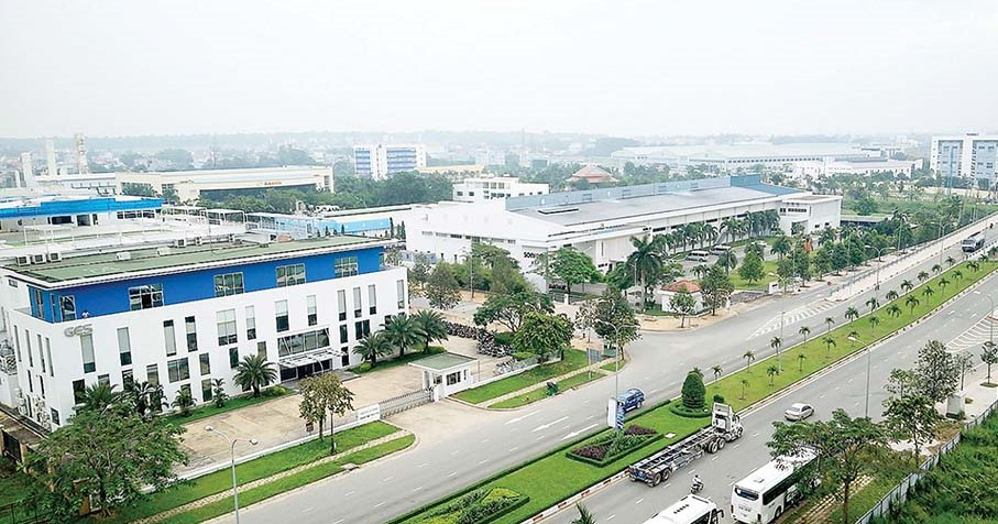
Back to the topic , in last 50 years , semiconductor industry have been all about the manifestation of Moore's law with respect to scal of integrated circuit. but as a consumer , what are the thing we would like to see in a electronics device .... first thing we look for is the cost and then we look for the features. But now it's close to saturation and we will not see much cost difference going forward as we saw in last 20 years .. where Nokia mobile phone comes around 15K INR and now same model you can get it in 2K INR ... its a huge difference.

The following (somewhat busy) slide from IBM summarizes things clearly saying: "Net: neither per wafer nor per gate showing historical cost reduction trends"

With increasing cost in capitals, process, R&D , design and manufacturing, it is really impossible to provide more cheap device with high features loaded.
There is one more reason the sharp increase of costs with scaling , in previous days, moving from one node (one technology like 40nm ) to other node , there were always cost associated with but as comparative , it was small.
What's coming in future ??
Think carefully and tell , what is the future of semiconductor ?? Design guys will get the design for next 5 or 8 years and once designs are there verification guys will also get the work .. for next 5 or 8 years atleast but then what will happen ? Will all design , verification , P&R guys sits ideal and waiting for new technology ?
There are saturation in all places , markets cracks and start from begin. But in semiconductor , there is no start from begin , people will have to think more deep and will have to come up with innovative ideas which will help to keep semiconductor industry moving.
People who are thinking to make career in this field , should think again. In 1995 , there were not many guys working in semiconductor , but from 2006/7/8 , many guys have started working in semiconductor domain .. after 5 years there will be many guys having 10+ years of exp ... what will be the scope for freshers that time ??
So My question is still there .... What coming next ???
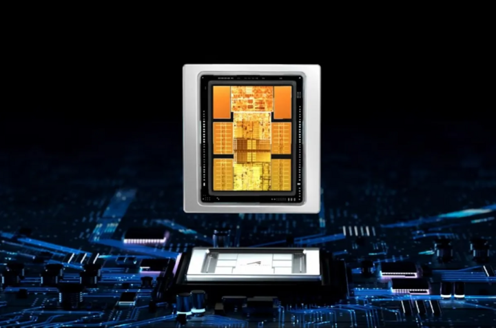
I think 28nm will be in market for next 3-5 years because 28nm TSMC is very good technology and full fill the designers dream to get their block working at high frequency without any timing issue .. but there are always limitation :) .
20nm,14nm, 10nm, 7nm are also an upcoming technology, one having interest can explore more on that.
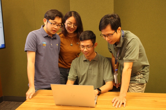
Bạn Có Đam Mê Với Vi Mạch hay Nhúng - Bạn Muốn Trau Dồi Thêm Kĩ Năng
Mong Muốn Có Thêm Cơ Hội Trong Công Việc
Và Trở Thành Một Người Có Giá Trị Hơn
Bạn Chưa Biết Phương Thức Nào Nhanh Chóng Để Đạt Được Chúng
Hãy Để Chúng Tôi Hỗ Trợ Cho Bạn. SEMICON